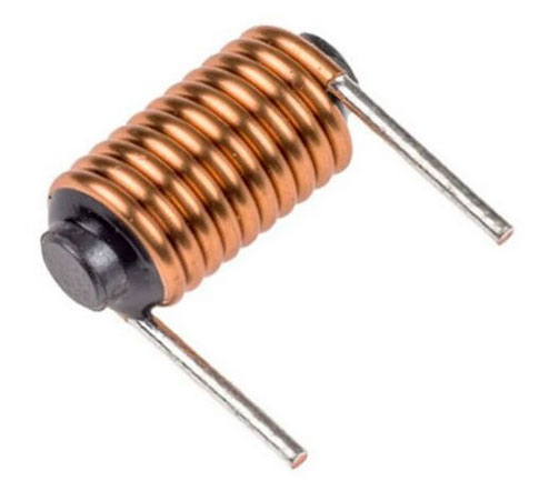
An inductor is a passive electronic component which is capable of storing electrical energy in the form of magnetic energy.
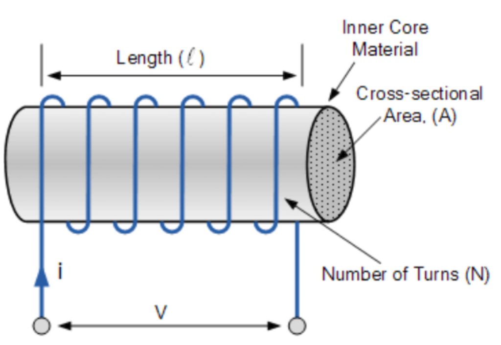
Any conductor of electric current (any wire for that matter) has inductive properties and can be seen as an ‘inductor’ and in order to enhance the ‘inductive effect’, a practical inductor is usually formed into a cylindrical coil with many turns of conducting wire.
Symbol
The voltage across an inductor is zero when the current is constant. In other words: An inductor acts like a short circuit for DC!
For the DC current, the coil acts as a piece of wire with a very low (almost zero) resitance. For AC current the coil acts as a resistor, combined with a capacitor.
An inductor is a component that can store energy in the form of a magnetic field. Another way to look at inductors is that they are components that will generate a magnetic field when current is passed through them, or will generate an electrical current in the presence of a changing magnetic field.
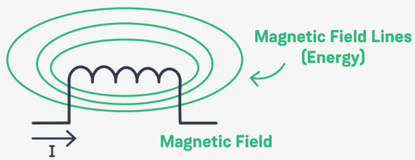
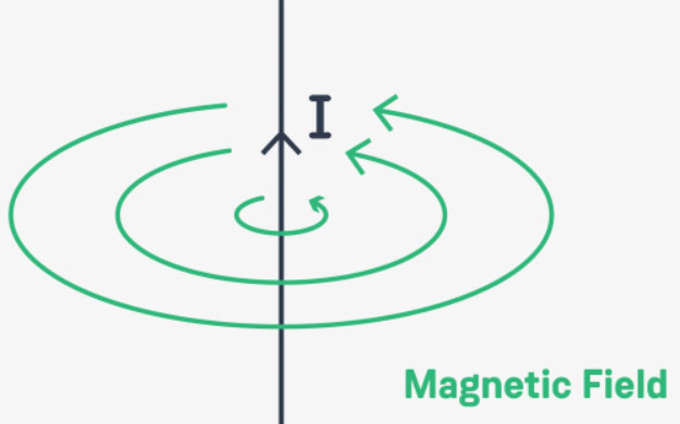
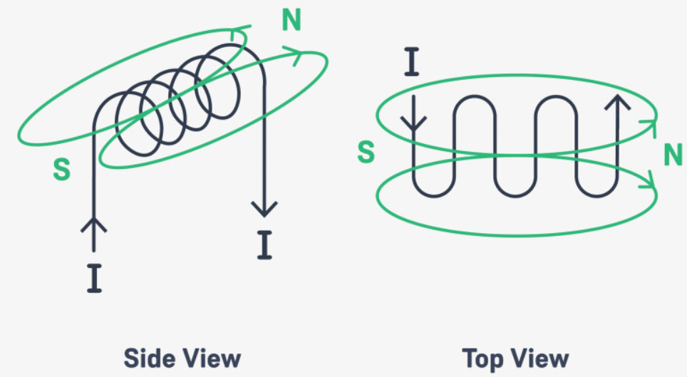
To explain exactly why inductors work the way they do is quiet complex – keep that in mind. Imagine a straight piece of wire (see below) -if we pass a current through, a circulair magnetic field is formed around it.
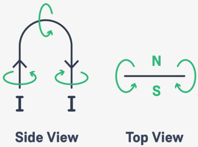
If we would bend this piece of wire, it shows that each side of the loop has fields in opposing directions. This is what creates our north- and south-pole on a electromagnet.
If we would add more loops we actually increase the number of magnetic rings being generated by the wire and therefore make a more powerful eletromagnet. In other words, we increased its inductance.
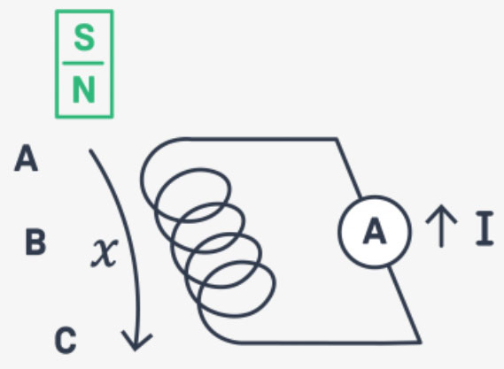
If we have a coil with no current flowing through it – the coil does nothing really. If we now would move a magnet through it, the changing magnetic field induces a current into the coil.
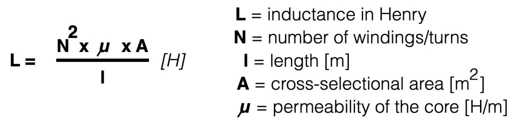
An example how the amount of inductance (measured in Henry [H]) can be calculated:
Coil with a ‘core’
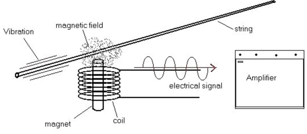
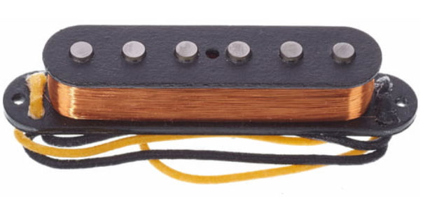
PickUp
A more common coil/inductor that we use is the ‘guitar-pickup’ for example. This pickup-coil consists of a permanent magnetic core inside the coil. By moving a string nearby the core of the pickup, a current is induced. See the picture below:
Guitar pickup
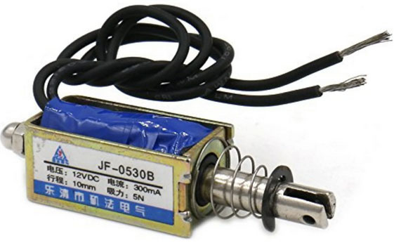
Solenoid
If you want to ‘move’ or ‘acuate’ an object, then a solenoid can be very practical to use. A solenoid is a coil (inductor) with a moveable iron core. If current is flowing through the coil, the iron core will be pushed out (or pushed in). See the picture below.
Solenoid
If the current stops flowing, the spring will push back the core. A practical application is opening the lock of doors for example.
OSC is a content format developed at CNMAT by Adrian Freed and Matt Wright comparable to XML, WDDX, or JSON.[2] It was originally intended for sharing music performance data (gestures, parameters and note sequences) between musical instruments (especially electronic musical instruments such as synthesizers), computers, and other multimedia devices. OSC is sometimes used as an alternative to the 1983 MIDIstandard, when higher resolution and a richer parameter space is desired. OSC messages are transported across the internet and within local subnets using UDP/IP and Ethernet. OSC messages between gestural controllers are usually transmitted over serial endpoints of USB wrapped in the SLIP protocol
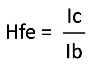
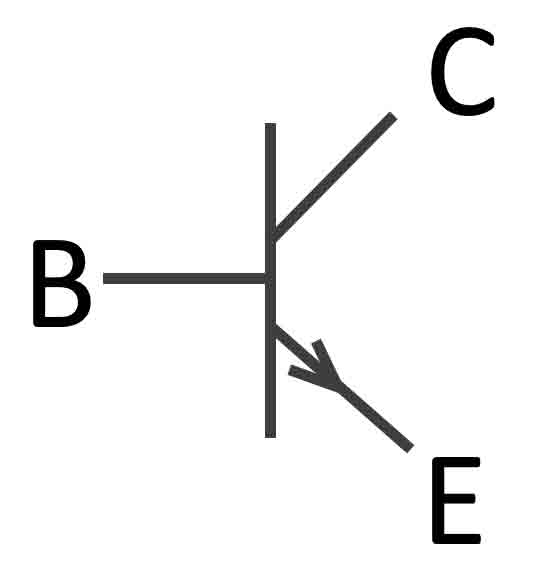
The invention of the transistor in the 1950’s changes the electronic world for ever. The transistor is a so called ‘semiconductor’ and is capable of amplifying signals. The transistor has a Collector (C), a base (B) and an emitter (E). It can be seen as a current controlled switch. A small current from the base to the emitter creates a bigger current (Ic) from the collector to the emitter. Take a look at this video-page, for a detailed explanation.
Imagine the transistoras the following setting: a large tube connected to a big pool of water. Halfway the tube there is a valve that can be changed position by a small tap on the side. Check figure 1.
If there’s no base current (ib=0) the transistor is closed and there’s no collector-current. If the base current Ib is increasing (we turn the small tap on the side – Ib > 0), the water-flow (=current or Ic) will increase as well. Check figure 2. If the Ib is maximum, the collector current Ic is at its maximum as well. The proportion between Ib and Ic is called the Hfe. This number represents the amount of current amplification.
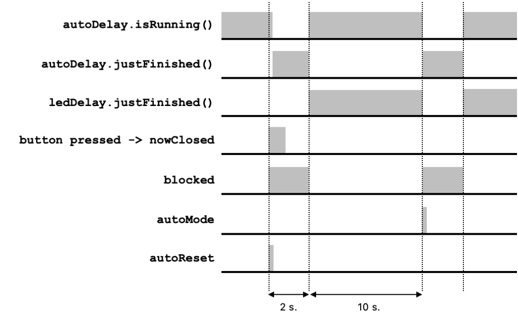
When movement is detected, this thing needs to go on for three seconds after which it should not be triggered for ten seconds. But if nothing happens in two minutes, it should trigger by itself. How?
Question posed by a random colleague student
The global behaviour of an installation based on a microcontroller, often includes timed processes. For instance, after a trigger, the input is blocked for a certain amount of time; if nothing happens for a while, generate an event; if within a certain time span a second trigger is sensed, change the behaviour; etc.
The most fundamental blink example suggests that timing can be controlled with a delay() function. However, the delay() has a fundamental issue which renders it useless in all of the situations described above: the program will proceed to the next line of code only when the wait is finished. In other words, during a delay(), all processing comes to a standstill. The function delay() could as well have been called holiday(). Therefore, ditch the delay().
The blink without delay and debounce examples introduce an approach to timing using the millis() function. It is an approach in which the passing of time is measured based on an onboard clock. When multiple overlapping time units are involved, this approach tends to become complex and difficult to manage. An alternative solution can be found in using the millisDelay statement, which is part of an external library. This library can be found and installed through the Manage Libraries… menu option.
Detecting State Change
In order to connect an action to sensor input, it is important to be clear about what is the difference between a sensor measurement—e.g. a value from digitalRead()—and a state changement—e.g. when a button is pressed, while before it wasn’t. Sensor measurement produces a stream of values, while a state change should be able to detect the moment at which a button is pressed. A stream of values is what is produced in the Digital Read Serial example.
In order to detect a state change, the code needs to be extended in such a way that the current state can be compared with the previous. When considering that what is defined in the loop() routine represents a single lifespan of the loop, something needs to be handed to the collective unconsciousness—or, in terms of Arduino code, a global variable—before the current run of the loop dies in order to be retained.
Here the order of things can be explained as follows. At the moment the button is pressed—nowClosed is true—while before it wasn’t—beforeOpen is true as well—the ifstatement checking these two booleans will execute the first section. The LED turns on and the serial monitor prints “switch closed”. At the moment the button is released, momentarily the else if sees it’s conditions met and will execute the connected block. All other cases are neither of these two options and are disregarded.
The last line—beforeOpen = !nowClosed—although it appears a bit cryptic is the crucial bit of information that becomes available the next time the loop runs: beforeOpen will become true if nowClosed is not true. We could consider this the will of the current loop that dictates the heritage of the next loop.
const int ledPin = 13;
const int switchPin = 2;
bool beforeOpen = true;


void setup() {
  pinMode(switchPin, INPUT_PULLUP);
  pinMode(ledPin, OUTPUT);
  Serial.begin(115200);
}

void loop() { // loop is (re)born
  bool nowClosed = digitalRead(switchPin) == 0;
  if (nowClosed && beforeOpen) {
    digitalWrite(ledPin, HIGH);
    Serial.println("switch closed");
    delay(5); // lazy debounce
  }
  else if (!nowClosed && !beforeOpen) {
    digitalWrite(ledPin, LOW);
    Serial.println("switch open");
    delay(5); // lazy debounce
  }
  beforeOpen = !nowClosed; // update global variable for next loop
} // loop dies
Temporarily Block Sensor Input
The state change introduced in the previous example, will be used here to connect specific actions. When the button is pressed, it will activate a timer that blocks the detection of the on state for a certain amount of time. Releasing the button will have no meaning in this context and the action connected to that can be removed.
The timer is created using the millisDelay.h library, and a delay is created using the millisDelay ledDelay statement. This ledDelay becomes a reference to a mechanic that is running in the background, that can measure time. A trigger is sent using ledDelay.start(LED_time), where LED_time specifies the amount of milliseconds it will take before ledDelay returns the trigger, signaling the end of the delay. This end trigger needs to be queried using the ledDelay.justFinished() statement, which will become true when this is the case. Until this happens, input by the button will be blocked.
A second millisDelay is added in order to automatically trigger the process—following the requirements posed in the top section, although for testing the time for this is reduced to 10 seconds.
When the Arduino starts up, this second delay, which refers to the autoMode flag, is triggered. Now there are two options, either the button is pressed before ten seconds pass, or isn’t. In the first case the autoDelay will be stopped; only when the button was pressed autoDelay.isRunning() will be true. Since later on in the code we will check whether the autoDelay.justFinished(), the autoReset flag is used to indicate that a reset has happened because of an activation, instead of time running out.
In the second case, the autoMode flag is raised so an activation can take place. The overview below shows how these flags are raised and lowered either because of a button pressed or the ten seconds auto trigger.
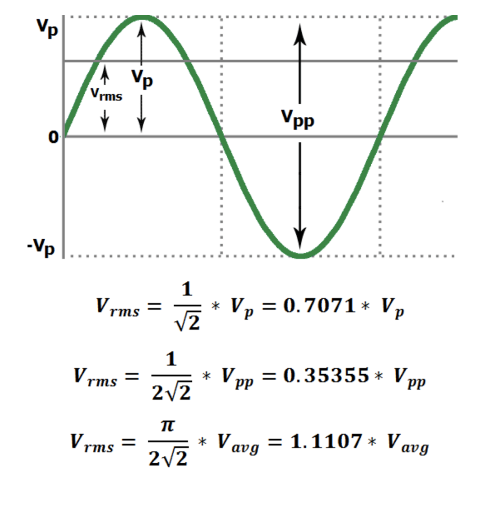
RMS Voltage Calculator (/calculators/rms-voltage- calculator)
This RMS Voltage calculator helps to 4nd the RMS voltage value from the known values of either peak voltage, peak- to-peak voltage or average voltage. It calculates the RMS voltage based on the given equations.
RMS (Root Mean Square) Voltage (Vrms)
Every waveform’s RMS value is the DC-equivalent voltage. Let’s take an example, if the RMS value of a sine wave is 10 volts then it means you can deliver the same amount of power via DC source of 10 volts. Do not confuse in between Average voltage and RMS voltage, as they not equal.
Peak Voltage (Vp)
A Peak voltage of a sine wave is measured from the horizontal axis (which is taken from the reference point 0) to the crest (which is the top or maximum voltage level) of the waveform. Peak voltage shows the amplitude of the waveform.
Vp = √2 * Vrms
By, this formula we can get the value Vrms of with respect to peak voltage.
Vrms = 0.7071 * Vp
Peak-to-Peak voltage (Vpp)
The difference between maximum peak voltage and minimum peak voltage, or the sum of the positive and negative magnitude of peaks is known as the Peak-to-Peak voltage.
Vpp = 2√2 * Vrms
By, this formula we can get the value of Vrms with respect to peak-to-peak voltage.
Vrms = 0.35355 * Vpp
Average voltage (Vavg)
The average value of a sine wave is zero because the area covered by the positive half cycle is similar to the area of the negative half cycle, so these value cancel each other when the mean is taken. Then the average value is measured by the half cycle only, generally we take the positive half cycle part for measuring.
The average voltage de4ned as “the quotient of the area under the waveform with respect to time”.
Vavg = 2√2/π * Vrms
By, this formula we can get the value of Vrms with respect to peak-to-peak voltage.
Grounding has a number of functions, a.o. safety, zero reference etc.. The combination of these functions can cause problems in the the audio chain when groundloops occur. This problem will be discussed in the underlying PDF.
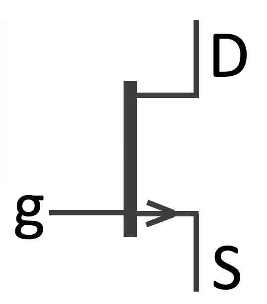
FET stands for Field Effect Transistor. It doesn’t behave like a BJT, it doesn’t amplify a base current. Instead a voltage on the gate (that hardly demands current) opens or closes the current in the source-drain. Hence, the input impedance of a FET can be very high (GOhm). It resembles therefore the behaviour of an electronic tube.
This chapter deals with a very important active component used in electronics. Since the implementation of the BJT (Bipolar Junction Transistor), sizes of electronic devices and computers could be shrinked enormously. e.g. In a modern CPU chip a few billion transistors are integrated. Basically a transistor is a (base)current amplifier. It can be used as a switch, a current amplifier , a voltage amplifier and many more things.
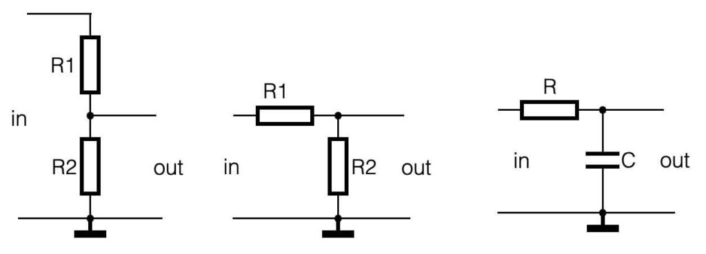
If we know that a capacitor act’s as a blockade (huge resistor) for DC ánd that the capacitor is a conductor (low resistance) for AC, we can make voltage ‘dividers’ that changes resistance and thus output voltage, at different frequencies.
If we combine a resistor and a capacitor in a series connection (the voltage divider for example), the behavior of that circuit changes because a time-constant is introduced.
R x C = time constant [seconds]
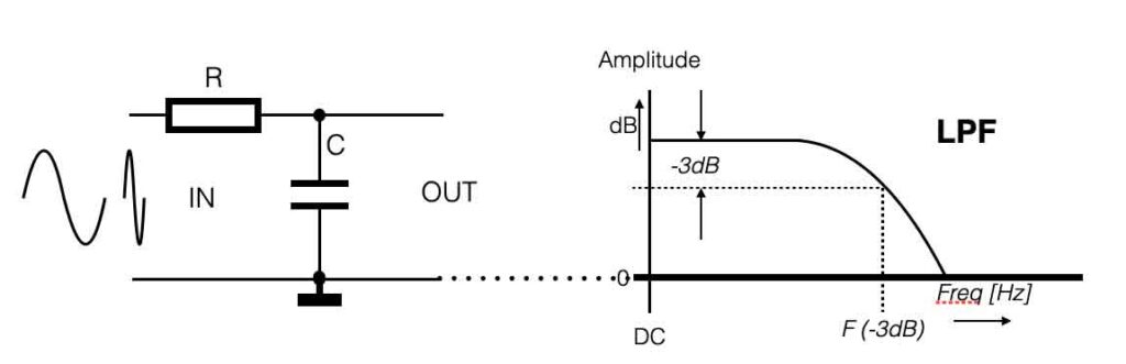
Low Pass Filter (LPF)
Take a look at the figure below. If we connect DC on the input of this RC-circuit, the capacitor will act a ‘infinite’ big resistor. The output will be equal to the input. If we change the input to AC, the resistance of the capacitor will change – it becomes lower. This means, the amplitude of the output will go down as well.
Passive Low Pass Filter
If we would give this filter a frequency ‘sweep’ (= change the frequency from low to high values), the voltage parallel to the capacitor (=output) will drop.
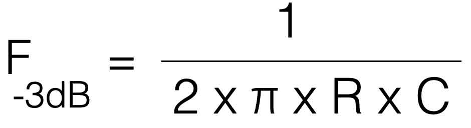
The frequency at which the output is half of the value of the input (this equals -3dB) is called the ‘cutoff frequency, F -3dB
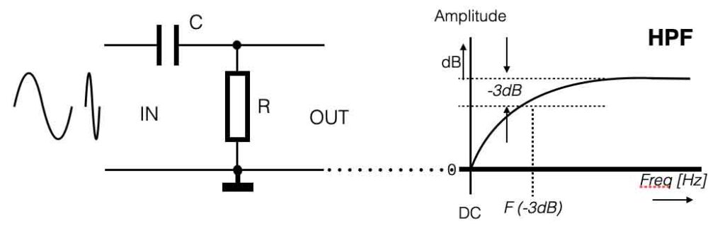
High Pass Filter (HPF)
If we change the position of the R and the C in this simple circuit, the behavior will change as well. Take a look at the picture below.
Passive High Pass Filter
If we start with DC as an input voltage (frequency = 0Hz), the capacitor acts as a very high resistance again. The output will therefor be low. Adding a sweep from low to high frequency will increase the output value. We introduced a High Pass Filter.